1. Introduction
The Waveform Generator has its origin in the research work on liquid crystals. It is thus optimized to produce, simultaneously in many channels, trains of pulses, each having its own duration, polarity and amplitude value. Typical arbitrary waveform generators are not well suited to this task since they were designed with quite different application in mind – generation of advanced analog functions, usually in one channel and at low voltage. Frequency and amplitude of such signals may be changed easily, but there is no easy and safe (for the connected device) way to alter the pulse trains during operation.
The generator has 8 channels and a common time base. The minimum pulse width is 150ns and the maximum amplitude is ±100 volts. The resolutions are 50ns and 50mV, respectively. The generator is controlled by a PC-Windows computer or Macintosh (OS9), taking advantage of the user-friendly operating system.
The waveform generator has the ability to change the applied waveforms during operation without transients. It has been accomplished by the use of two memory banks.

Mathematical relations between pulses in the waveforms and between different time-steps can be programmed-in to avoid repeated, manual adjustments of many pulses each time the waveforms should be altered. The waveforms may also be grouped for simultaneous amplitude adjustments, as for example, row and column electrodes in a matrix display.
2. General Concept
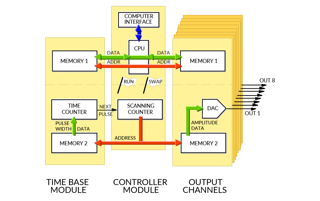
Undisturbed waveform modification during operation is based on the incorporation of two memory sets. When the data from one memory set are used for the waveform synthesis, the other memory set can be freely updated. After successful updating, the memory sets are interchanged (swapped) immediately after completing the generation of the old waveform.
It is, thus, possible to consider the waveform generator as consisting of two, fairly independent, parts: a microprocessor system associated with one memory set and a hardware- controlled waveform-synthesis circuitry (Figure 1). Here, the second memory set is scanned by an address counter at a rate defined by the timing module. Obtained data are then transformed into a corresponding voltage level by a digital-to-analog converter (DAC) and a series of operational amplifiers.
Waveforms are not synthesized from equidistant points. Instead, there is a 15-bit width data associated with each individual pulse number. In other words – each time slot can have individual width.
3. Controller Module
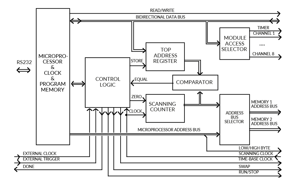
The central device in the controller module is a Motorola 68HC11F1CFN4 microprocessor. It communicates with the host computer by a standard serial port. Received commands and data are used to update the currently associated memory on the designated module (or modules). They are also stored in own “note-pad” memory, since identical updating must later be performed on the other memory set in order to bring both sets to identical state.

Both memory sets have separate address busses. The address-bus selector block connects one of them to the microprocessor’s address bus and the other to the scanning counter. The ‘memory swapping’ is performed by interchanging the above address bus assignments and forcing the modules to make corresponding change in their data-selector blocks. Swapping does not cause any delay.
The relation between the microprocessor address lines and the address inputs of the memory circuits is not straightforward. The microprocessor’s lowest address line, A0, is used as ‘Low/High-Byte’ control signal, which activates one of the two memory circuits. The memories’ address inputs are, thus, shifted up by one bit, and the RAM_A0 inputs are connected to the microprocessor’s A1 line, RAM_A1 to A2, and so on. Since the memories on all modules occupy the same address space, the microprocessor has to use the module-access selector functional block to aid choosing the desired memory circuit to communicate with. The specific memory circuit is, thus, chosen by three signals: module-select (the board), swap (the memory set) and low/high byte (the circuit). The data may be written into a few modules at once, if so desired.
While one memory set is associated with the microprocessor, the second one gets its addresses from the scanning counter, which counts from zero upwards (unless REVERSE direction is activated). The counter is driven by the scanning clock delivered from the timing module. The value, generated by the scanning counter, is compared with the address of the last waveform-pulse data, stored in a top address register. When the end of the waveform is reached, the comparator sends the ‘equal’ signal to the control logic block, which, in turn, checks if the microprocessor flags out for memory swapping or for terminating the waveform generation. If the memory swap is requested, then the ‘swap’ control-signal is inverted and the top address register is updated to the prepared value (because the waveform length might have been changed). The counter is then reset to zero and the new scan begins.
The control-logic block takes also care of some additional functions. It prepares the time-base clock, senses the external start-signal (if enabled), and supervises the operating mode, which may be either continuous, burst (i.e. the waveforms are generated once only) or other special modes.
4. Timer
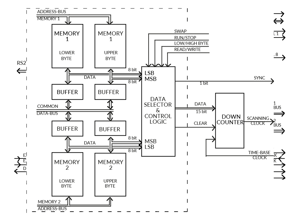
The duration of each pulse is defined by a timing module (Figure 3). Here, a 15-bit data is loaded to a down-counter at the beginning of each waveform step. The counter is driven by a time-base clock, the speed of which is selectable and may be 1 or 20 Mhz (crystal controlled), a slower, software-controlled clock (in 1 ms steps) or an externally supplied one (should be less than 20 MHz but can be very slow). The output of this counter produces a scanning clock, which, in turn, advances a memory-address counter.
The 16th data bit contains arbitrarily placed trigger information, used to synchronize an oscilloscope (or other device) with the desired step of the waveform.
5. Data Memories
The part of the block scheme from Figure 3, enclosed in the dashed rectangle, is present both in the timing module and all analog-output modules. It consists of the memories, buffers, a data selector and a control logic, and its purpose is to deliver 16-bit data to the counter or, in the case of the analog-output channel, to the DAC.
Since the microprocessor operates on 8-bit data bytes, a conversion to the required 16-bit data words is needed. Thus, each memory set consists of two 8k*8 random-access memories, which store the lower and upper byte of the 16-bit data word, respectively. The memories are tied to the microprocessor data bus through a programmable logic device (CPLD). Normally, the buffers of the CPLD are in the high-impedance state (disabled), effectively disconnecting the memories from the data bus. When a specific memory circuit is selected by the microprocessor (in the previously described way), the control logic activates the corresponding buffer. The direction of data flow is then defined by the microprocessor’s read/ write signal.

The buffers associated with the memory set being scanned are always disabled. The memories are, thus, isolated from the microprocessor activity and the data may be delivered undisturbed through the data selector to the DAC.
6. Digital-to-Analog Conversion
The process of conversion of binary data into the analog signal is crucial for the obtainable speed and amplitude. We use a 14-bit digital-to-analog converter DAC904U settling within 30 ns. The current output from the DAC is converted to a voltage by a fast operational amplifier OPA690. This signal is fed to a high-voltage amplifier PA98.
The DAC uses twelve bits (b11…0) out of sixteen data bits available, that gives 50 mV resolution of the pulse amplitude at the high voltage output. The sixteenth bit (b15) may be set via software and is provided as TTL-level output on the front panel. It may be used for other purposes, like controlling external devices.
Two isolated BNC contacts for high voltage (±100V) output are provided on the front panel of each module, since one usually connects both the load and the oscilloscope probe to the same signal. If the load is connected between two outputs (as in the case of a liquid crystal cell) one needs to monitor the difference between the two applied signals. For this purpose two summation modules are provided. The summation module has one inverting (-IN) and one non-inverting (+IN) inputs which can accommodate the ±100V signals from high-voltage outputs of the generator. The output of the summation module is low voltage in the range ±10V, low power and intended for oscilloscope only.
7. Programmable Logic Design
All digital logic is incorporated into programmable logic devices – CPLDs from Lattice.
8. Options
The generator is controlled through a standard serial interface and different computers or programs may be used in order to adapt the system to specific requirements. The communication protocol and commands are described at the end of this manual. This allows also to control the generator using LabView or similar software. It is advisable to contact Pendulum Instruments for the latest listing before programing a dedicated driver. Do not hesitate to contact the company when specific needs arise as it may be possible to adapt the software or hardware of the generator.