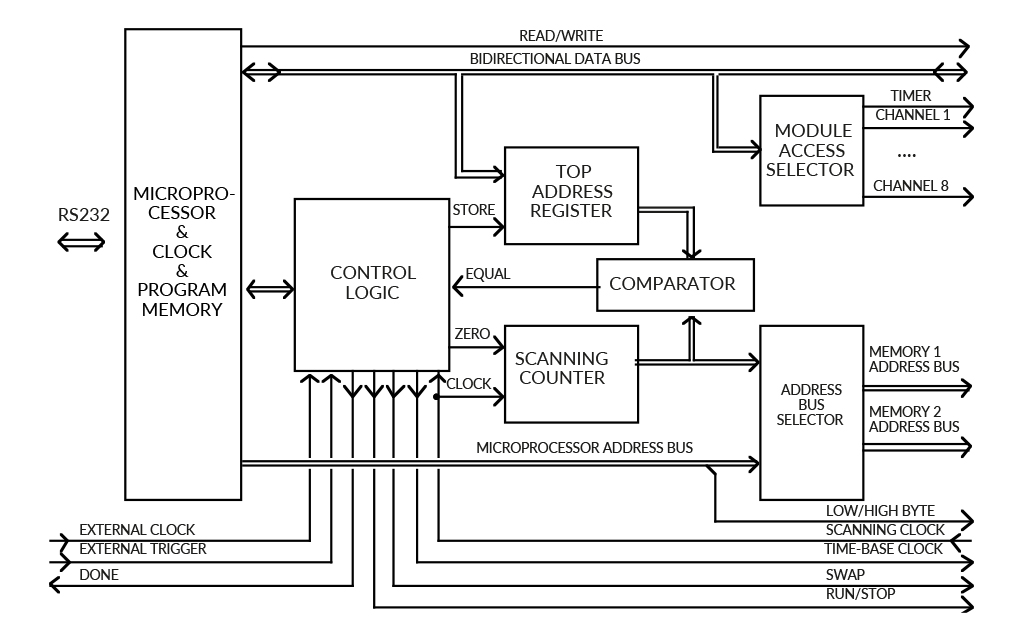
The central device in the controller module is a Motorola 68HC11F1CFN4 microprocessor. It communicates with the host computer by a standard serial port. Received commands and data are used to update the currently associated memory on the designated module (or modules). They are also stored in own “note-pad” memory, since identical updating must later be performed on the other memory set in order to bring both sets to identical state.

Both memory sets have separate address busses. The address-bus selector block connects one of them to the microprocessor's address bus and the other to the scanning counter. The ‘memory swapping’ is performed by interchanging the above address bus assignments and forcing the modules to make corresponding change in their data-selector blocks. Swapping does not cause any delay.
The relation between the microprocessor address lines and the address inputs of the memory circuits is not straightforward. The microprocessor's lowest address line, A0, is used as ‘Low/High-Byte’ control signal, which activates one of the two memory circuits. The memories’ address inputs are, thus, shifted up by one bit, and the RAM_A0 inputs are connected to the microprocessor's A1 line, RAM_A1 to A2, and so on. Since the memories on all modules occupy the same address space, the microprocessor has to use the module-access selector functional block to aid choosing the desired memory circuit to communicate with. The specific memory circuit is, thus, chosen by three signals: module-select (the board), swap (the memory set) and low/high byte (the circuit). The data may be written into a few modules at once, if so desired.
While one memory set is associated with the microprocessor, the second one gets its addresses from the scanning counter, which counts from zero upwards (unless REVERSE direction is activated). The counter is driven by the scanning clock delivered from the timing module. The value, generated by the scanning counter, is compared with the address of the last waveform-pulse data, stored in a top address register. When the end of the waveform is reached, the comparator sends the ‘equal’ signal to the control logic block, which, in turn, checks if the microprocessor flags out for memory swapping or for terminating the waveform generation. If the memory swap is requested, then the ‘swap’ control-signal is inverted and the top address register is updated to the prepared value (because the waveform length might have been changed). The counter is then reset to zero and the new scan begins.
The control-logic block takes also care of some additional functions. It prepares the time-base clock, senses the external start-signal (if enabled), and supervises the operating mode, which may be either continuous, burst (i.e. the waveforms are generated once only) or other special modes.