The part of the block scheme from Figure 3, enclosed in the dashed rectangle, is present both in the timing module and all analog-output modules. It consists of the memories, buffers, a data selector and a control logic, and its purpose is to deliver 16-bit data to the counter or, in the case of the analog-output channel, to the DAC.
Since the microprocessor operates on 8-bit data bytes, a conversion to the required 16-bit data words is needed. Thus, each memory set consists of two 8k*8 random-access memories, which store the lower and upper byte of the 16-bit data word, respectively. The memories are tied to the microprocessor data bus through a programmable logic device (CPLD). Normally, the buffers of the CPLD are in the high-impedance state (disabled), effectively disconnecting the memories from the data bus. When a specific memory circuit is selected by the microprocessor (in the previously described way), the control logic activates the corresponding buffer. The direction of data flow is then defined by the microprocessor's read/ write signal.
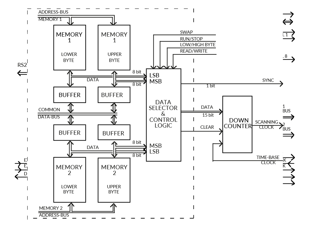
The buffers associated with the memory set being scanned are always disabled. The memories are, thus, isolated from the microprocessor activity and the data may be delivered undisturbed through the data selector to the DAC.